


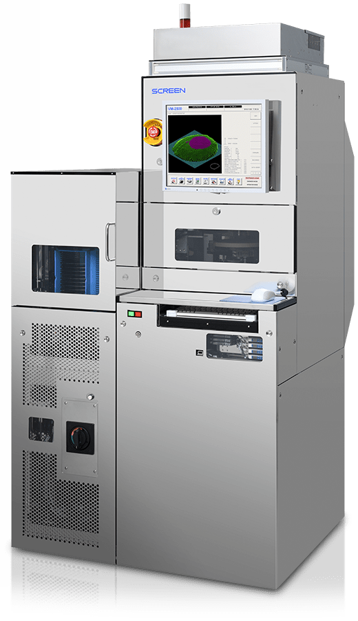

 Our proprietary transfer mechanism and ellipsometry/spectroscopy-based processing ensure stable, high-precision transport and measurement of a wide range of wafers.
 Our systems also handle special wafers and ultra-thin films. Specifications are available to satisfy most operation and installation space requirements.
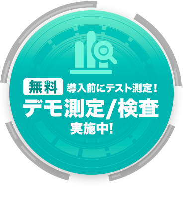
 Please use our free wafer measurement demonstrations to inspect the accuracy of our products.


 Inquiries:
Please contact us via the application form for demonstration requests
Inquiries:
Please contact us via the application form for demonstration requests
 We will be in touch:
Our sales/technical staff will respond to your inquiry (this service is available face-to-face or as an online/phone correspondence)
We will be in touch:
Our sales/technical staff will respond to your inquiry (this service is available face-to-face or as an online/phone correspondence)
 Wafer delivery
Please send the wafers in once the conditions are decided based on our consultation.
Wafer delivery
Please send the wafers in once the conditions are decided based on our consultation.
 Measurement process
We will perform the measurements after receiving the wafers.
Measurement process
We will perform the measurements after receiving the wafers.
 Data delivery
The measurement data will be returned to you approximately 2 weeks after we receive the wafer.
Data delivery
The measurement data will be returned to you approximately 2 weeks after we receive the wafer.
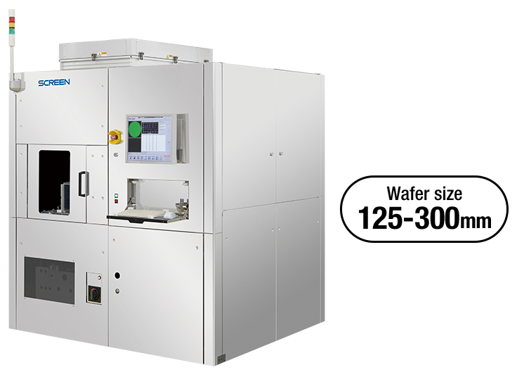

A high-end model capable of high precision minute measurements as small as 40 μm square, simultaneous measurements of film thickness and optical constants, while achieving twice the throughput of conventional systems. Optional installation of a single wavelength ellipsometer is available.

The VM-2500 and 3500 are ideal for in-plane, multi-point measurement of communication and other devices. Both deliver up to 160 wph (SiO2, 5-point measurement) and also features log storage and improved maintenance support.

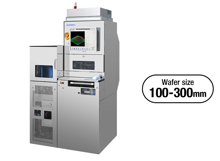
Equipped with CCD image sensors enabling simultaneous measurement across all wavelengths of the visible light spectrum, supporting precise, high-speed measurement of film thicknesses. Added wizard function for easier recipe creation, and increased the number of recipes managed and registered.
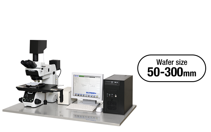

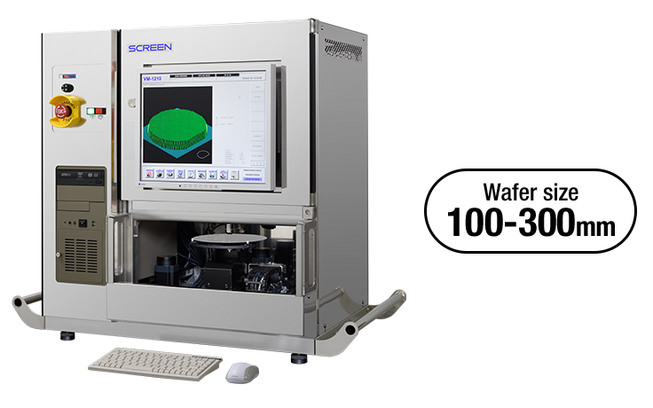
Composed of a microscope section and spectrometer section that incorporates a lens unit, manual XY stage, electric revolver, objective lens, filter insert section and light source. The spectrometer also features a fibre optic input type CCD, making the system more compact, enabling fast, highly precise measurement.
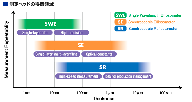
■SWE: Single Wavelength Ellipsometer
The SWE uses a long-life laser diode as a light source, which helps reduce running costs, and provides a high-precision measurement of thin films with a thickness of 20 nm or less
■SE: Spectroscopic Ellipsometer
These units enable simultaneous measurement of film thickness and optical constants. Particularly suitable for processes where film quality management is just as crucial as the development of thin film materials and deposition processes.
■SR: Spectroscopic Reflectometer
Our SR units can handle up to four layers of laminated films. Visible light and UV light are both available, allowing target films to be measured under the most appropriate conditions.
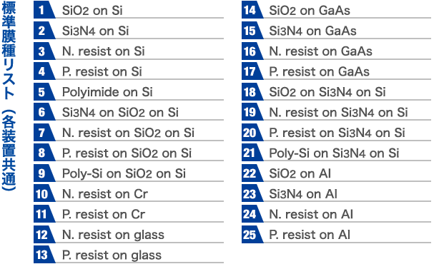
Each system comes with 25 standard film recipes. Operators can add their customized versions enabling special compound wafers to be processed and improving measurement work flexibility.
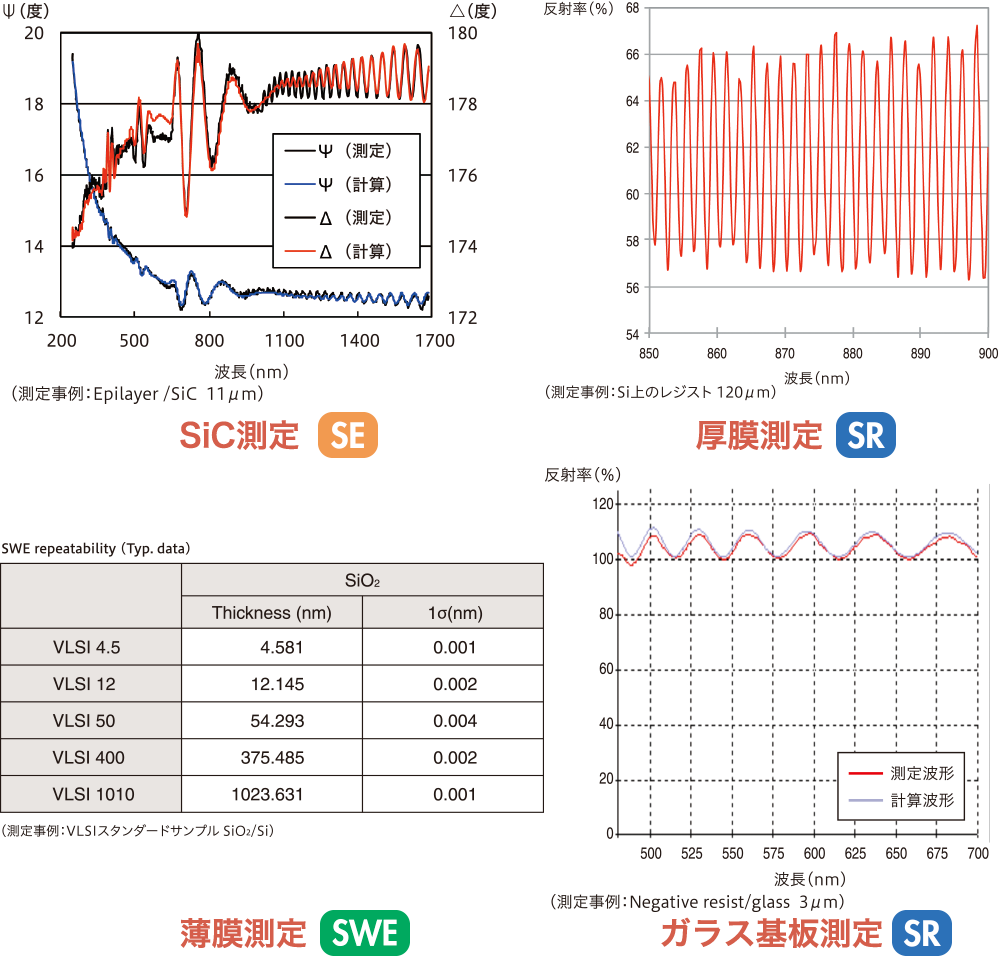
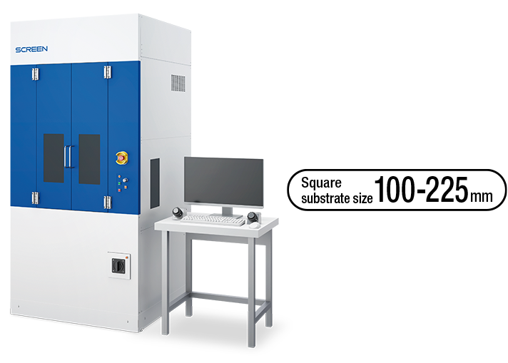
Preloaded with measurement applications to fully satisfy a wide variety of needs. Includes infrared spectrum analysis for thickness measurement of SiC epilayers, which is difficult to achieve with visible light. Capable of measuring thick, thin, laminated and PZT / GaN films as well as glass substrates, square substrates and panels.

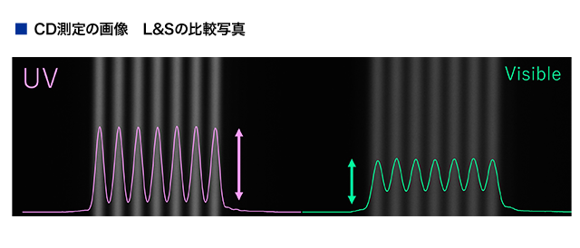
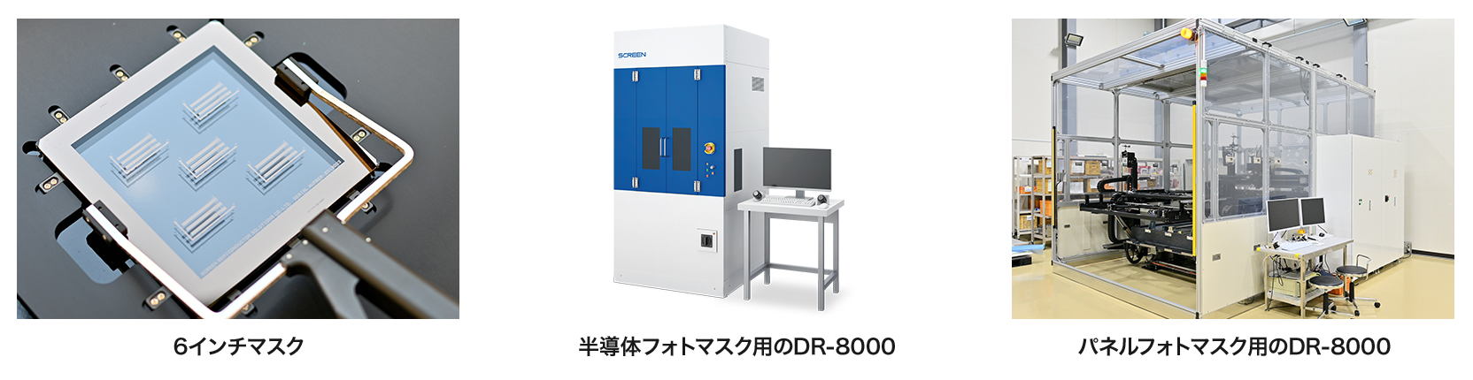
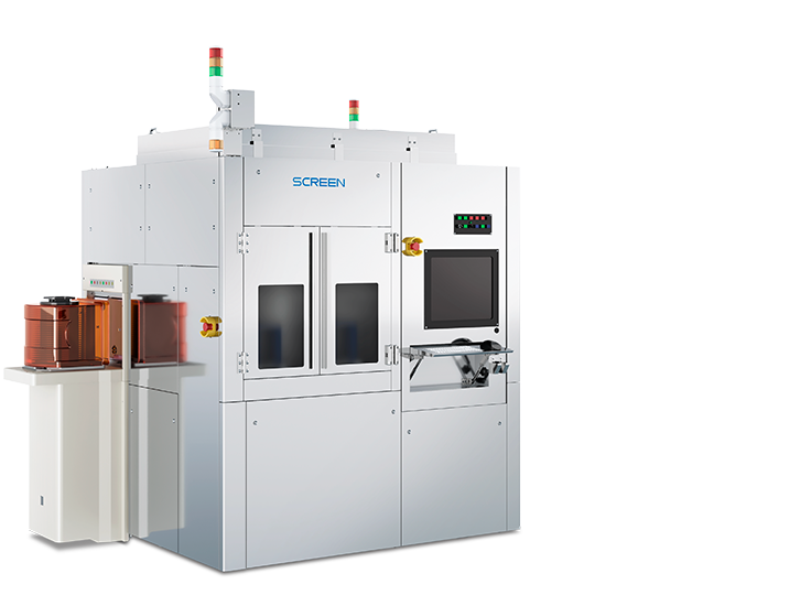
Photomasks are the original plates used to transfer circuit patterns, so photomask quality greatly impacts final product quality. The DR-8000 is able to measure the line widths, or critical dimensions (CDs), of intricate circuit patterns with high nano-order accuracy and repeatability. In addition to the CD measurement function, the DR-8000 can also be equipped with functions for measuring transmittance and phase shift, both key parameters for intricate circuit patterns, and for observing the aerial image during exposure, which is essential for photomask development and quality assurance.
■CD measurement
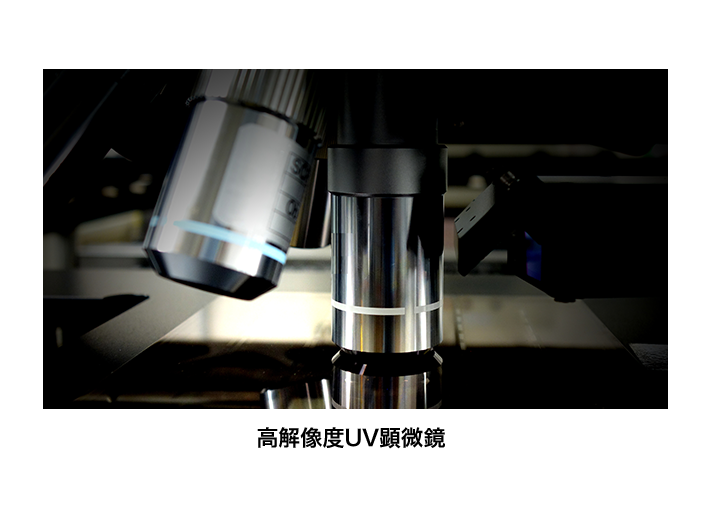
A dedicated UV objective lens specially designed for CD measurement and uniform UV transillumination ensures high resolution and reliability. Consistent and accurate measurements are achieved thanks to a powerful edge determination algorithm and SCREEN’s unique focus system.
SCREEN has developed a multi-edge CD measurement function that enables measurement of a variety of designs, including line and space (L&S), hole, and resist patterns, as well as mask patterns having complex optical profiles with unique characteristics in the pattern film structure.
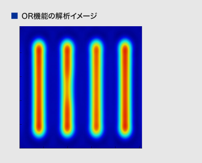
■OR function (measurement of aerial images)
An OR (optical reader) function performs observation and measurement of aerial images when transferring circuit patterns using photomasks. The OR function uses light of the same wavelength as the exposure system and enables setting of the exposure system parameters “NA” and “σ”. The transfer result at the time of exposure is simulated using light without having to use the exposure system. For example, by precisely measuring the intensity and dimensions of the aerial image to assess transfer performance during exposure, it is possible to quantitatively evaluate pattern defects.
■Phase shift measurement function
A phase shift mask is a semiconductor miniaturization technology that utilizes a light interference effect. Measuring the amount of phase shift, which is an index of interference, is essential for quality assurance of phase shift masks. The DR-8000 uses SCREEN’s unique double-slit method to measure the phase shift at the exposure wavelength. Combining a unique algorithm with one-shot image acquisition of the double slit interference fringes enables highly accurate phase shift measurements.
■Transmittance measurement function
Facilitates measurement of the transmittance of halftone, phase shift, and other masks. Use of an LED light source with exceptionally stable intensity combined with light source intensity correction technology ensures high repeatability (3 σ: 0.1% or less).
■Review function
Enables defects to be reviewed at high resolution based on the coordinate data output from the defect detection system. This review can also be performed for photomasks after pellicle attachment.
We have a wealth of experience in handling substrates other than photomasks. Demos/evaluations using wafers and glass substrates can be provided. Please feel free to contact a SCREEN representative.
■Lineup
Photomasks for semiconductors:Compatible with quartz glass and soda lime glass photomasks (4, 5, 6, 7, and 9 inches)
Photomasks for large panels:Handles large photomask substrates (G6, G8, and G10) with a proven track record for transfer using industrial robots
Special applications
Wafers (example): 100 to 300 mm in diameter (transparent or opaque)
Glass substrates (example): 600 x 600 mm


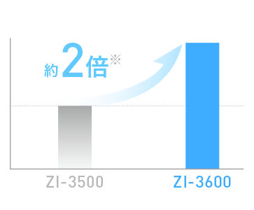
The ZI-3600 provides precise, high-speed pattern inspection regardless of wafer size and the number of chips. The incorporated three lenses and the use of recipes allow for an easy switch between resolutions.
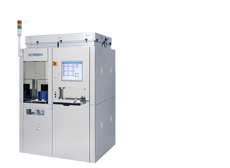

New wafers can be inspected immediately through this highly flexible model with easy-to-create recipes. The proprietary inspection head and high-speed image processing engine handle fast and reliable inspections.
The ZI-3600 ensures stable production through the use of line sensor inspection, executing entire wafer surface checks at a constant speed regardless of the size of the wafer and the number of chips.
* Compared to our ZI-3500 model
Inspection conditions can be set with ease while checking images of the actual wafers. Thanks to this feature, any operators can create recipes even if they are not specialized engineers.
Critical dimension and overlay measurement can both be added as optional functions. Simply set the required conditions when creating a recipe to perform line and space and overlay measurements in a single step.
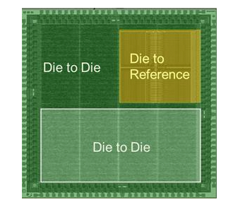
Three types of inspection methods – die to die, cell to cell, and die to reference – can be freely combined and set in the same recipe. Alternatively, a non-pattern inspection can be performed.

Test measurements and inspection services of your specified wafer are available prior to installation.
We also welcome you on-site for a face-to-face consultation in our Kyoto office.
Please contact us with any inquiries!